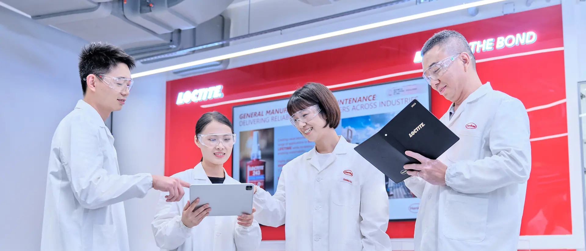
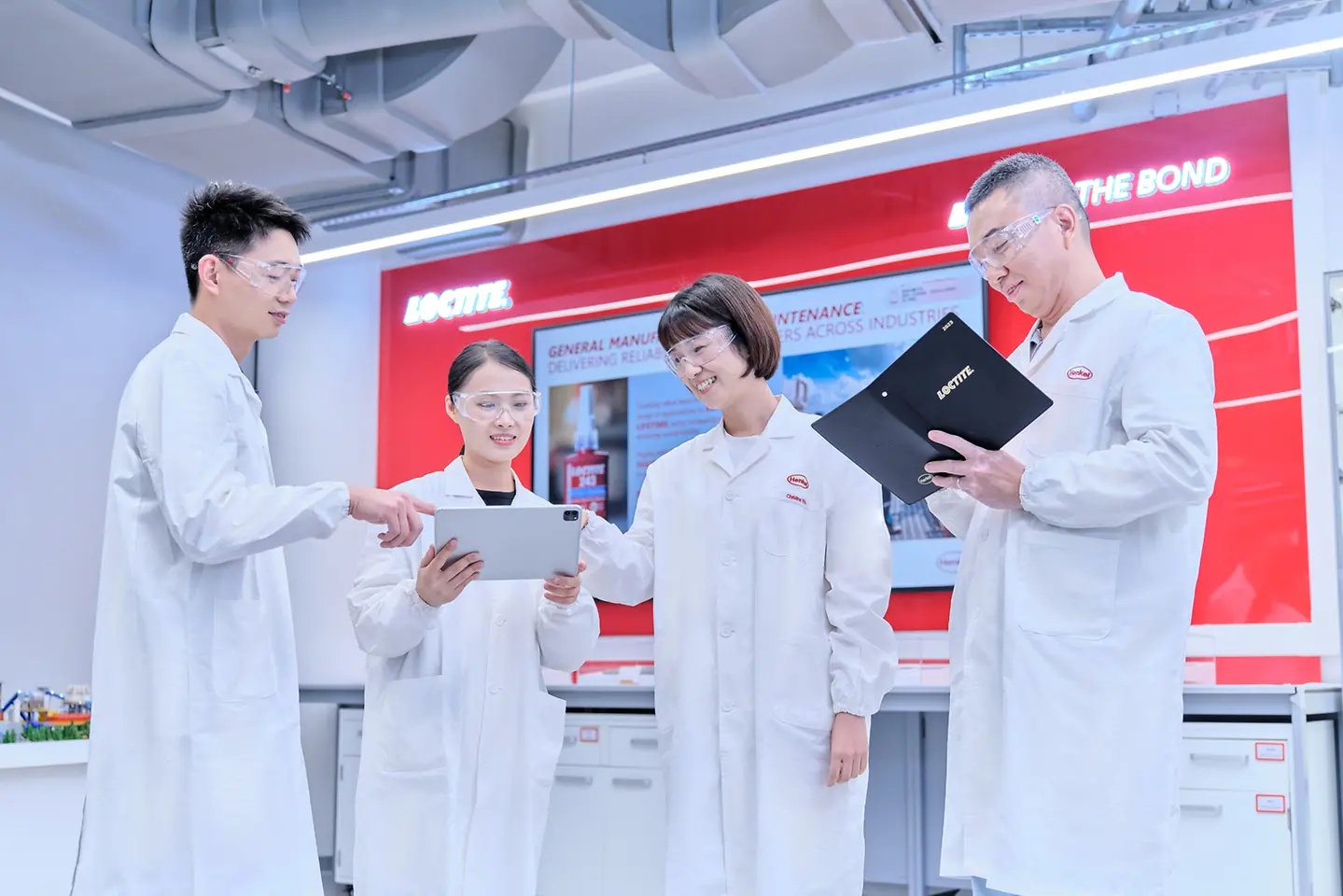
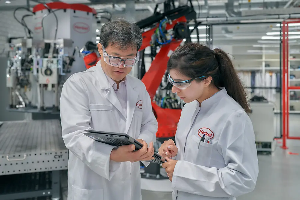
At Henkel Adhesive Technologies, we believe that collaboration is key to driving innovation.
INSPIRATION CENTER SHANGHAI
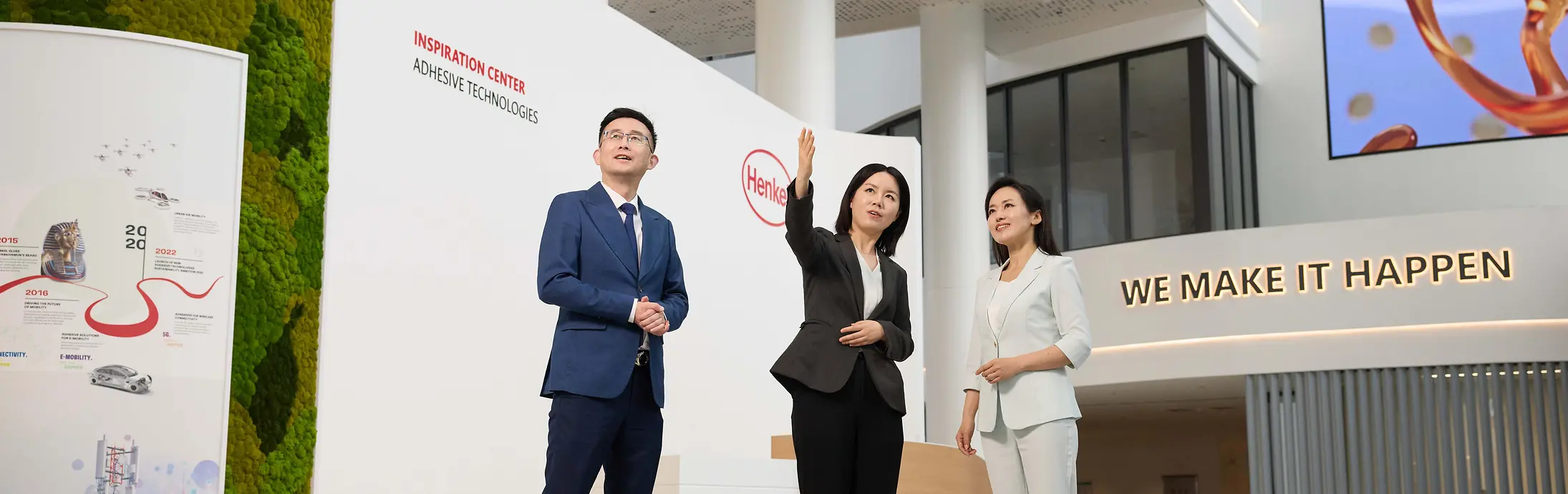
Experience our state-of-the-art facilities, groundbreaking technologies, inspiring working environment, and our long-lasting partnerships during your Inspiration Center Shanghai (ICS) visit.
DRIVING INNOVATION THROUGH COLLABORATION
At the Inspiration Center Shanghai (ICS), we are shaping the future of adhesive technologies by providing customer-centric solutions: This is where we welcome customers, industry partners, and academia to collaborate with our experts and develop innovative and sustainable technologies for the Asia-Pacific region.
Interact with our experts at an event, get inspired on a customized tour, and innovate with us in a workshop to take your business to the next level.

BOOK YOUR VISIT
Are you looking for innovative technology solutions? Would you like to learn from other applications and be supported by an experienced partner? Then we invite you to book your visit to the Inspiration Center Shanghai.
1 of 2
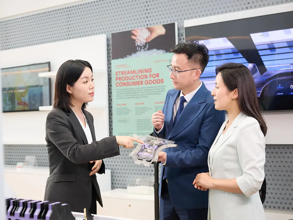
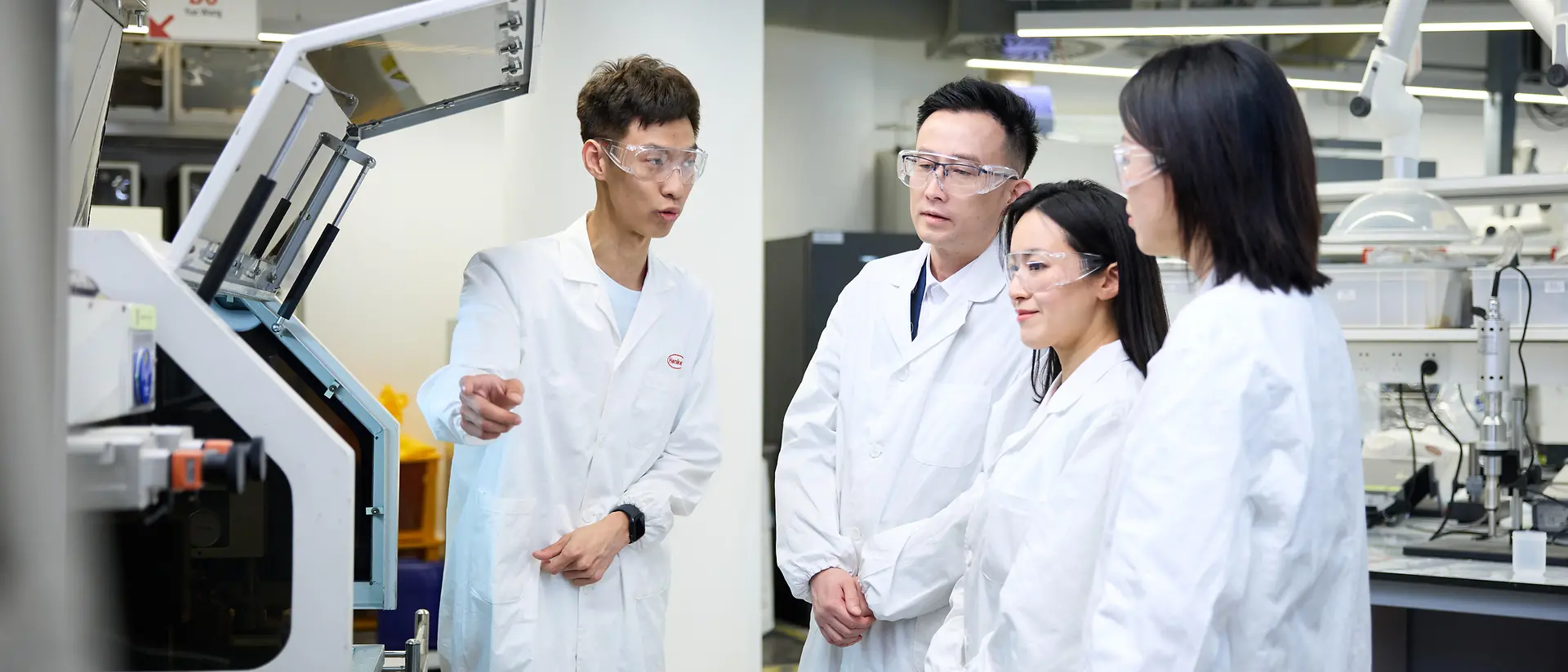
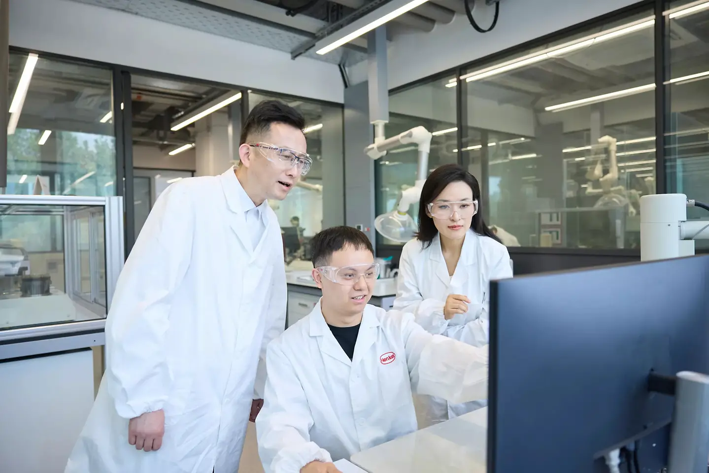
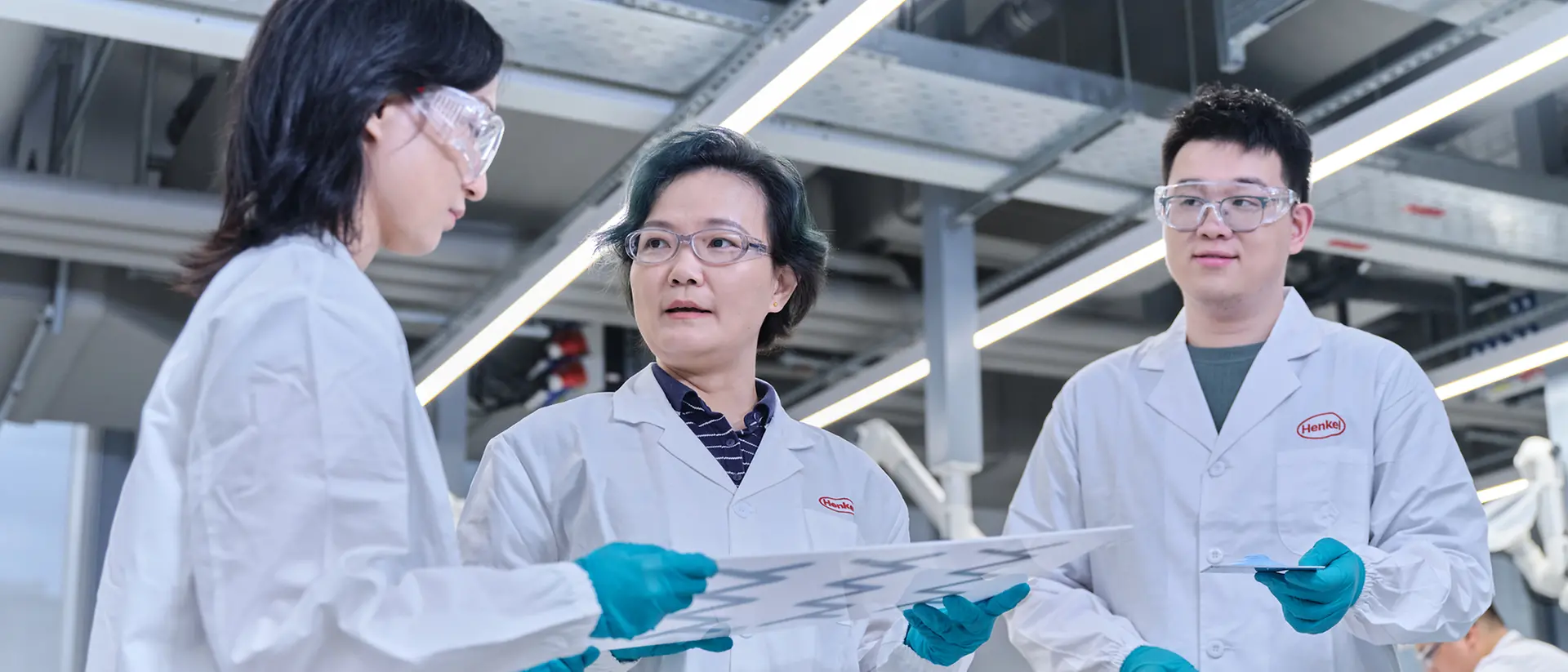
CUSTOMER EXPERIENCE


LABORATORIES
Automated Lab & Certification Testing Center
Critical Infrastructure & Machinery MRO Lab
Printed Electronics Technology Lab
Analytical Material Testing Lab
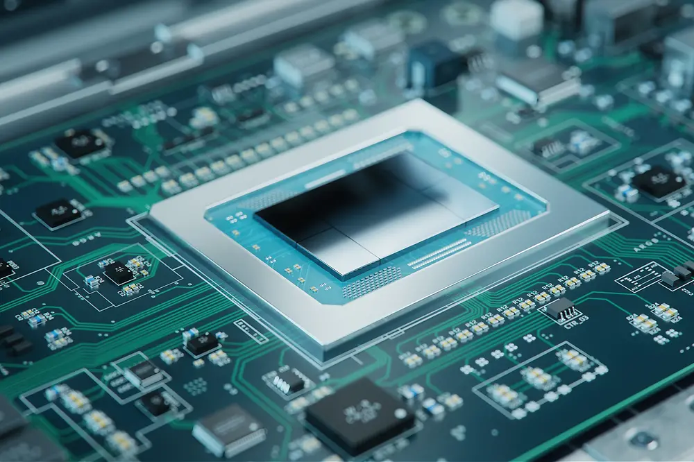
Semiconductor Testing Lab
Thermal Management Lab
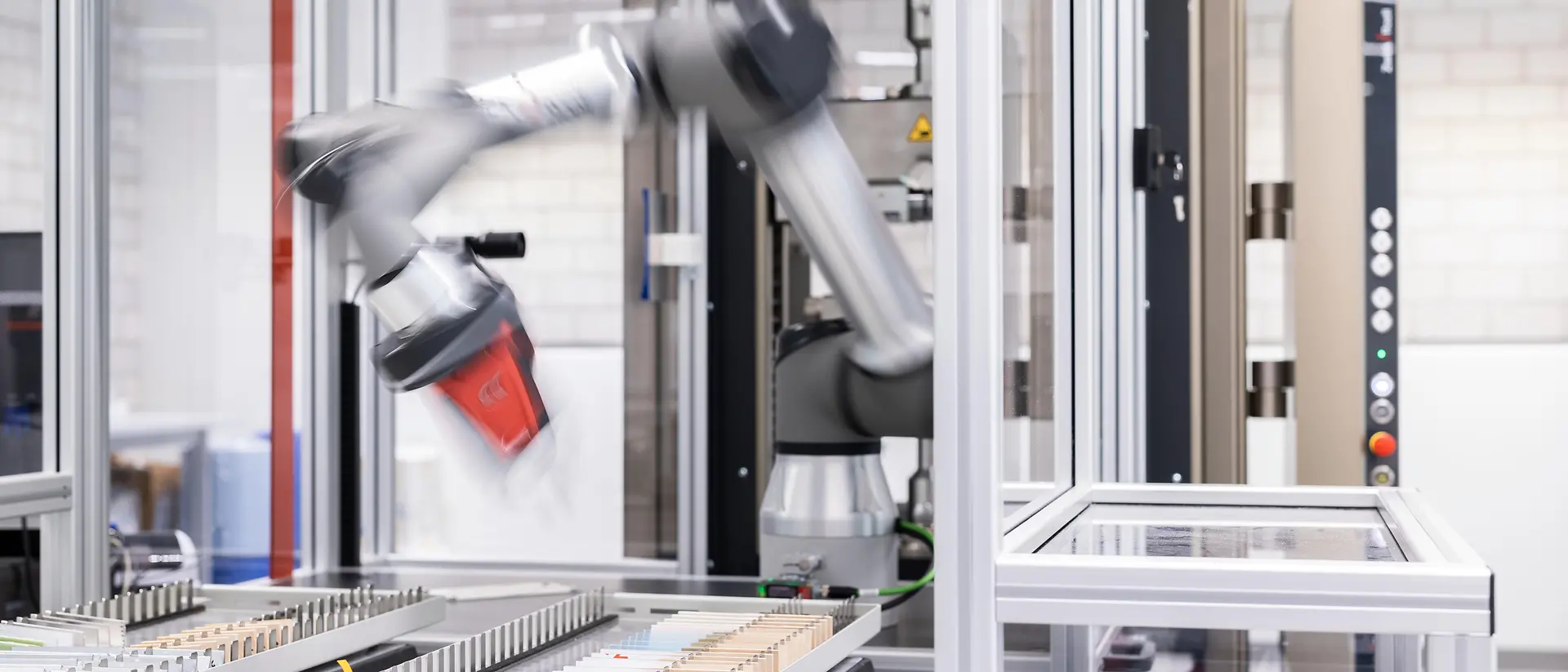
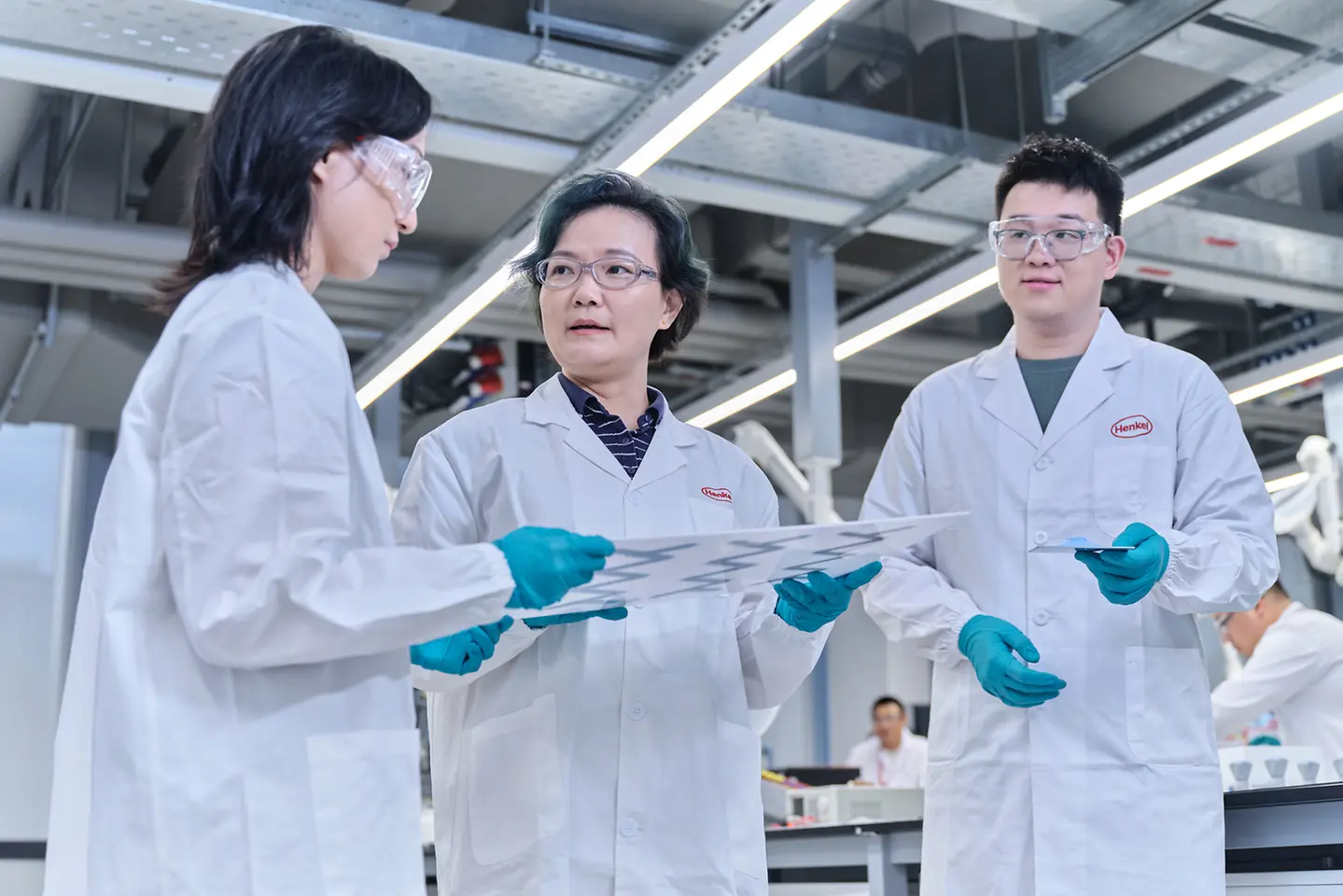
Discover the Automated Lab, a cutting-edge, data-driven laboratory that seamlessly prepares, tests, and screens new formulations. Connected to the Automated Lab is a cloud-based digital platform that captures the entire material development process. Each function facilitates the collection and analysis of clean, harmonized data, thereby enabling shorter development timelines.
In this lab, you will see the industrial leading products and solutions to help customers to better secure their critical infrastructure and machines to extend their life, increase efficiency, and improve reliability.

Discover how we create data-driven solutions through formulation, printing, and innovation in the Printed Electronics Technology Lab. Our printing technologies include 3D printing, printed electronics, and electrically conductive adhesives (ECAs). In this lab, we transform new design ideas into digital 3D and 2D manufacturing innovations by leveraging Henkel's advanced materials science and automation capabilities.
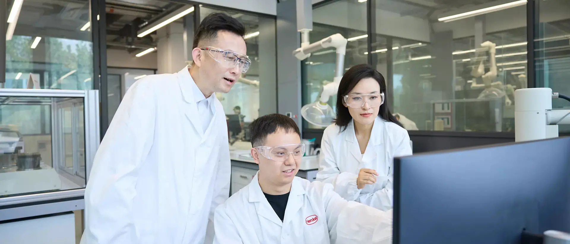
This lab focuses on specialized skillsets of instrumental analysis to enable Henkel’s innovation competitive advantage. The lab provides cross-industry support with first-class analytical expertise and comprehensive instrumental capabilities. Our capabilities include among others surface, chromatography, mass spectrometry analysis as well as material characterization.
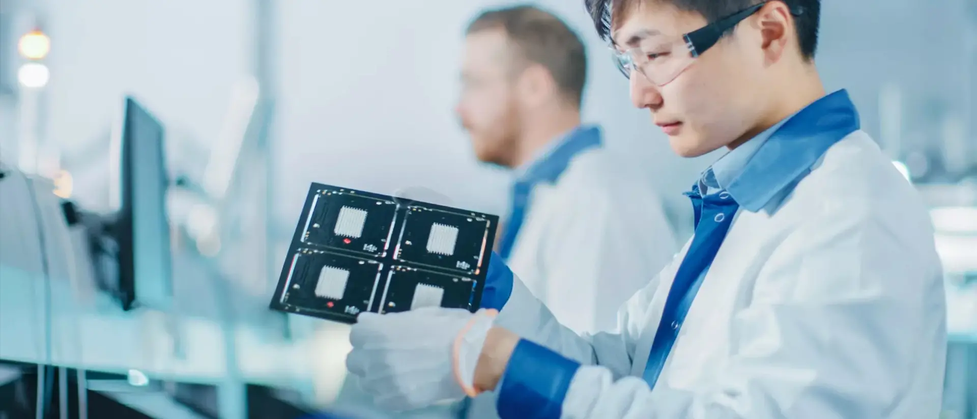
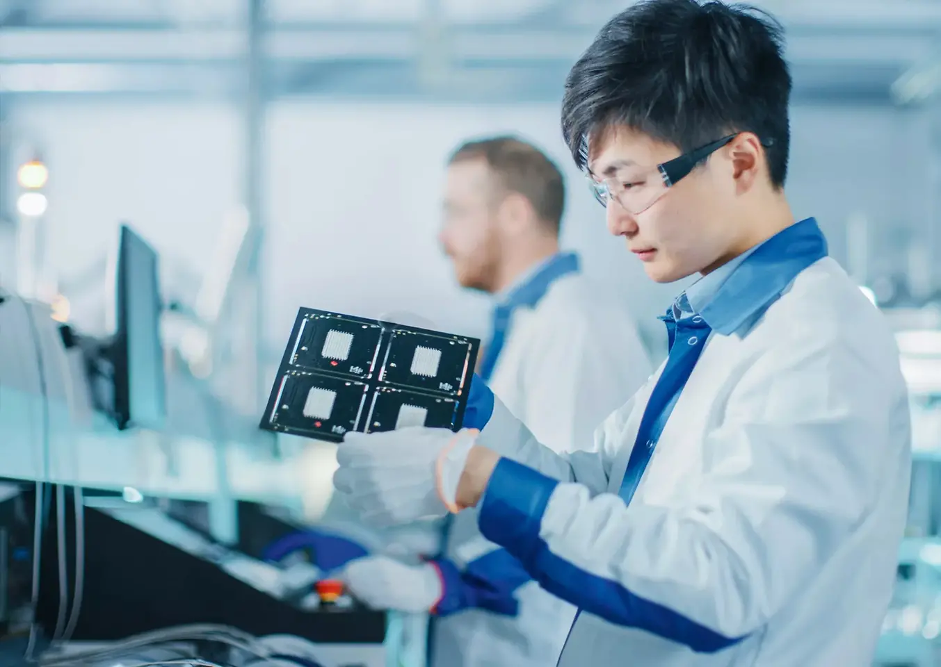
This lab is dedicated to the development of semiconductor materials and their applications, with a strong focus on driving innovation in semiconductor technology. Its core mission is to explore the properties of emerging semiconductor materials and processes, develop advanced manufacturing techniques, and identify their potential applications across a wide range of semiconductor devices to address customer pain points. Through in-depth analysis and rigorous experimentation, the lab aims to deliver more efficient and reliable solutions that meet the increasing demands for performance and energy efficiency in modern semiconductor packaging.
Discover how we create next-generation thermal management solutions through formulation, testing, and innovation in the Thermal Management Lab. This lab focuses on the research and development of future-oriented thermal conductive materials including gels, pads, gap fillers and phase change materials in multiple fields such as automotive, industry and electronics.
Automated Lab & Certification Testing Center
Discover the Automated Lab, a cutting-edge, data-driven laboratory that seamlessly prepares, tests, and screens new formulations. Connected to the Automated Lab is a cloud-based digital platform that captures the entire material development process. Each function facilitates the collection and analysis of clean, harmonized data, thereby enabling shorter development timelines.
Critical Infrastructure & Machinery MRO Lab
In this lab, you will see the industrial leading products and solutions to help customers to better secure their critical infrastructure and machines to extend their life, increase efficiency, and improve reliability.
Printed Electronics Technology Lab
Discover how we create data-driven solutions through formulation, printing, and innovation in the Printed Electronics Technology Lab. Our printing technologies include 3D printing, printed electronics, and electrically conductive adhesives (ECAs). In this lab, we transform new design ideas into digital 3D and 2D manufacturing innovations by leveraging Henkel's advanced materials science and automation capabilities.
Analytical Material Testing Lab
This lab focuses on specialized skillsets of instrumental analysis to enable Henkel’s innovation competitive advantage. The lab provides cross-industry support with first-class analytical expertise and comprehensive instrumental capabilities. Our capabilities include among others surface, chromatography, mass spectrometry analysis as well as material characterization.
Semiconductor Testing Lab
This lab is dedicated to the development of semiconductor materials and their applications, with a strong focus on driving innovation in semiconductor technology. Its core mission is to explore the properties of emerging semiconductor materials and processes, develop advanced manufacturing techniques, and identify their potential applications across a wide range of semiconductor devices to address customer pain points. Through in-depth analysis and rigorous experimentation, the lab aims to deliver more efficient and reliable solutions that meet the increasing demands for performance and energy efficiency in modern semiconductor packaging.
Thermal Management Lab
Discover how we create next-generation thermal management solutions through formulation, testing, and innovation in the Thermal Management Lab. This lab focuses on the research and development of future-oriented thermal conductive materials including gels, pads, gap fillers and phase change materials in multiple fields such as automotive, industry and electronics.
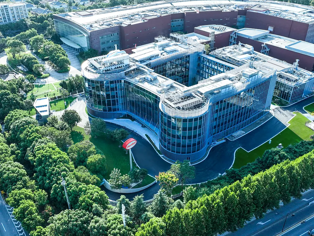
INSPIRATION CENTER SHANGHAI
IN A NUTSHELL

>500 employees working in 32 labs

33,000 m2 spread over 6 floors

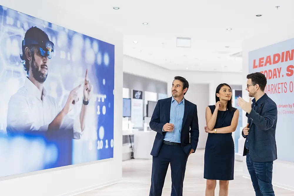
270° digital experience in the Infinity Room

~48,000 mechanical tests carried out in the Automated Lab
1 of 4
VISIT OUR INNOVATION CENTERS
IN OTHER REGIONS

EXPLORE HOW
WE DRIVE INNOVATION
Our success stories highlight how we develop and drive ideas forward. Read more about the megatrends that inspire us and discover how we make a positive impact across industries and applications.

1 of 3